
Building a 3-Phase Servo Motor Driver
In the past few months I was intensively exposed to servo motors: their constructions, working principles, and driving circuits, thanks to my internship. These motors are brushless, driven by 3-phase AC currents, and when properly controlled (as in my internship company), can execute motion with nanometer-level of resolution. The science and technology behind these motors deeply fascinated me, which inspired me to try building my own 3-phase servo motor driver, one of the core components in the motor’s control.
The 3-phase servo motor driver is essentially a 3-phase DC-to-AC converter, which provides current measurement and feedback for control purpose. The major functional blocks of the driver are as follows:
- 3-Phase MOSFET inverter and MOSFET gate drivers.
- Phase Current Sensing.
- Power Supply System.
- Feedback Signal Conditioning & ADC (Optional).
In addition, this driver will also provide complete isolation between high-power circuit and MCU control circuit (MCU control circuit is external to the driver).
The 3-Phase Inverter
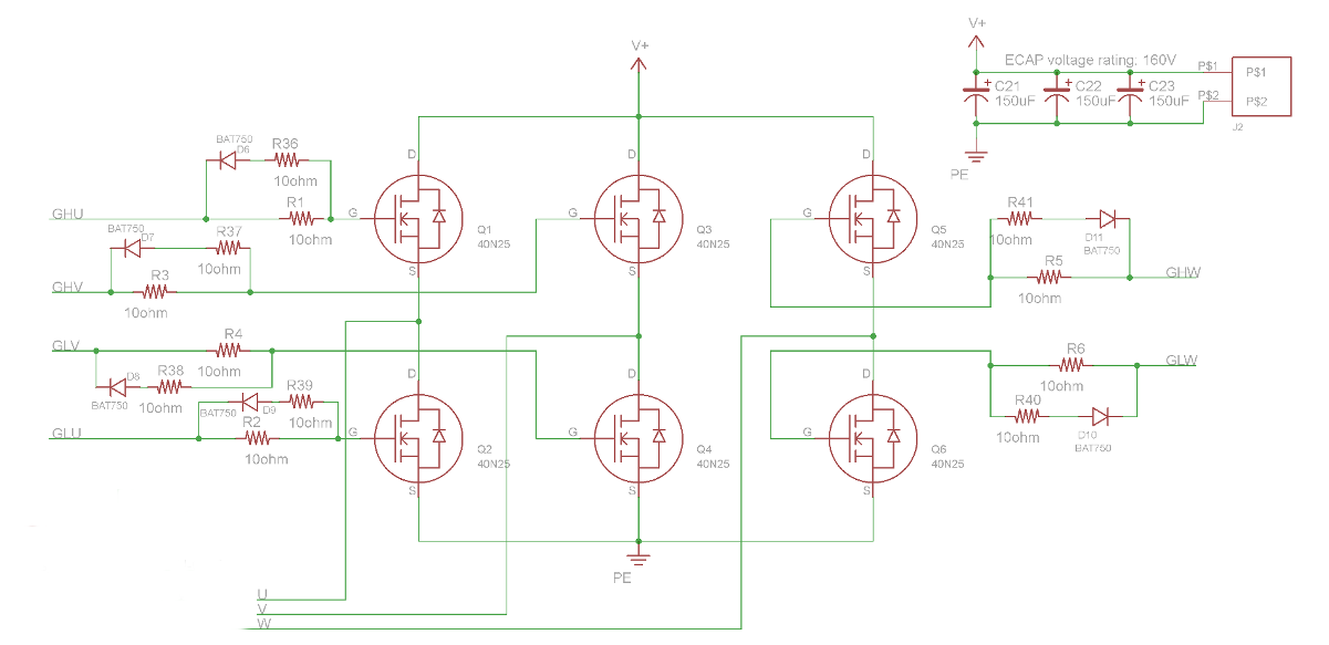
The 3-phase inverter circuit consists of 3 half-bridge circuits, which controls the 3 phases of the motor. Each half-bridge is made up of 2 MOSFETs (I used Fairchild 40N25). the inverter circuit is shown in Fig.1. The inverter is powered from V+, which is the motor’s power supply with user-defined voltage (according to needs, max 100V DC).
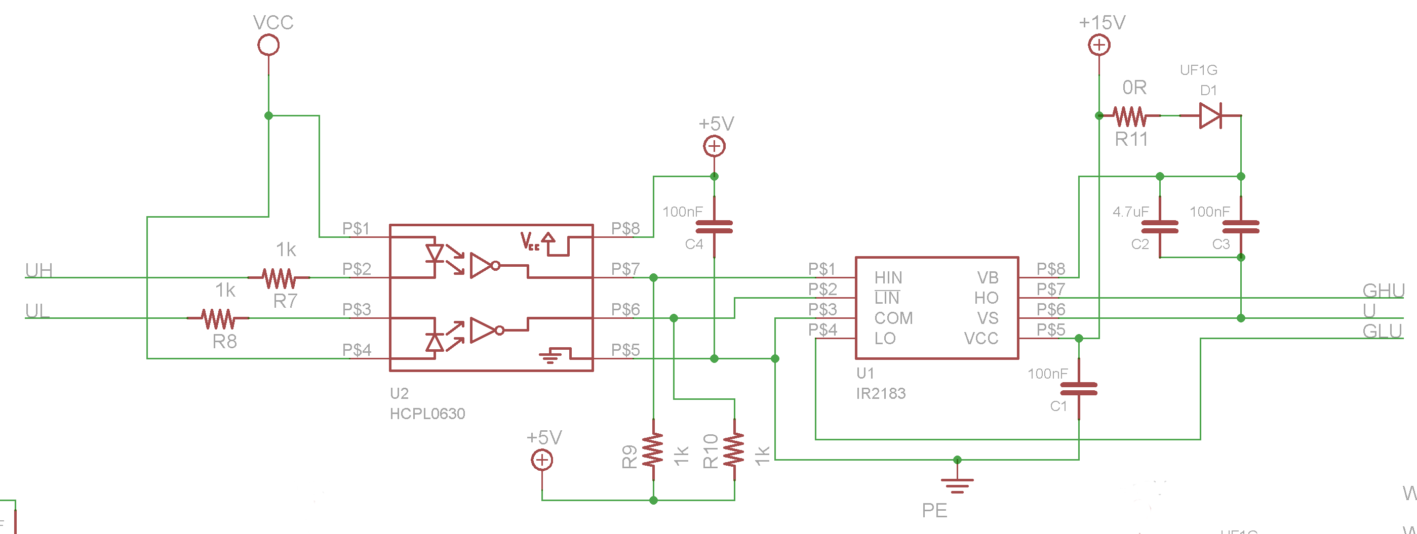
Because both high- and low-side of the half-bridge uses N-channel MOSFET, and becuase of the characteristics of N-Channel MOSFET, a gate driving circuit becomes necessary. I used IR2183 integrated half-bridge driver to do this job. The driver circuit (for one phase only) is shown in Fig.2. Opto-coupler HCPL0630 was used to isolate the high-power driver circuit from MCU. Sorry but please notice that value of R7 and R8 shown in Fig.2 (1K ohm) is WRONG because I misunderstood some datasheets. The value for R7 and R8 in the final design is 330 ohm.
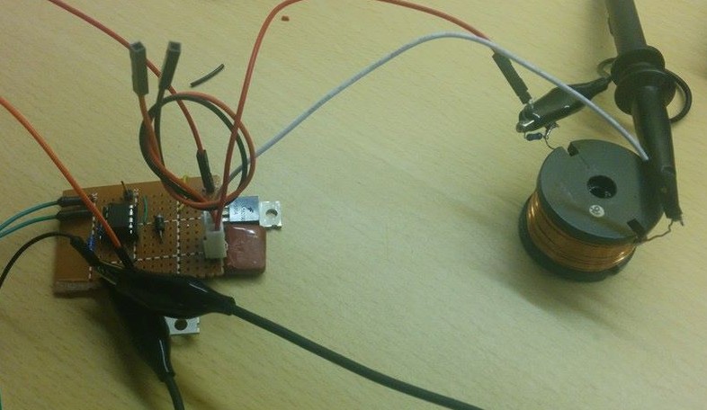
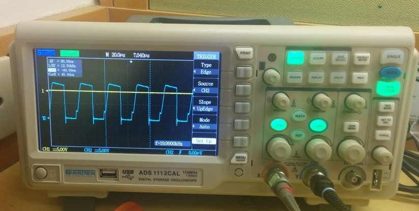
To make sure the design works, I built a prototype of the inverter circuit (1 phase only) and tested it (shown in Fig.3 and Fig.4). Fig.4 shows the halg-bridge switching an inductive load with approx. 70% duty. The MOSFET gate driver circuit (Fig.2) does not operate when PWM duty is below approx. 3% or above approx 95%.
Phase Current Sensing
The job of the current sensing circuit is to accurately measure the amount of current flowing in each phase. The measurement is then provided MCU, which executes a close-loop control algorithm that controls the current flow in phases (the current loop). I used LTSR-25NP current transducer to sense the phase currents. LTSR-25NP is a hall-effect current censor, and its output is completely isolated from the current that it measures. It helps isolate high- and low-power parts of the driver board.
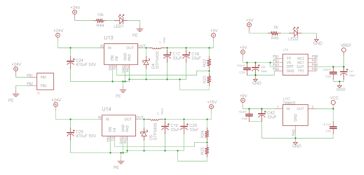
Power Supply System
In my driver, the motor is powered from V+ (user-defined, max 100V DC). However, the rest of the system: MOSFET gate drivers, current sensors, etc, are powered from a separate power source, fixed at 24V DC. This 24V voltage is converted by switch-mode voltage regulators into 2 different voltages:
- 15V: power supply to MOSTEF gate drivers
- 5V: for high-power circuits that needs 5V supply (e.g. opto-isolator, high-power side).
In addition, there is another 5V linear regulator, which supplies power for low-power circuits that needs 5V: opto-isolator low-power side, current transducers, etc.
An additional 5V voltage, VREF, is provided by REF195 (by Analog Devices). this is the precision voltage reference for an the onboard ADC (which was never tested, sadly)
The power supply curcuit is shown in Fig.6.
Feedback Signal Conditioning & ADC
to be added
PCB Design
My driver board features 4-layer PCB, with middle layers dedicated to GND and power supply. In the layout I paid attention to keep the ground panel for high- and low-power circuits separated. Total isolation is achieved by using opto-isolators and isolated current sensors. The Layers are shown in Fig.7 ~ Fig.10, and the completed PCB is shown in Fig.11(front side) and Fig.12(back side).
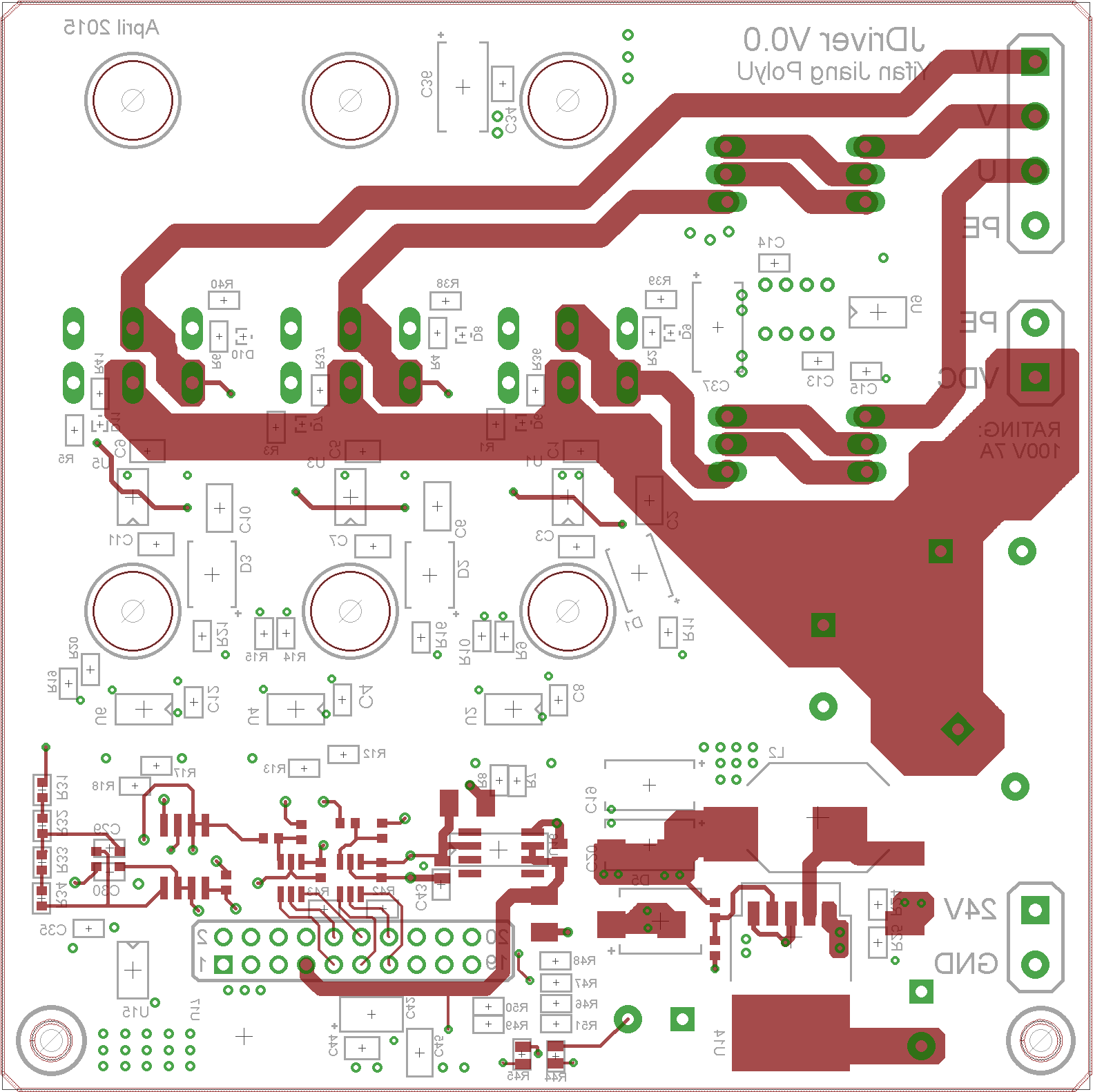
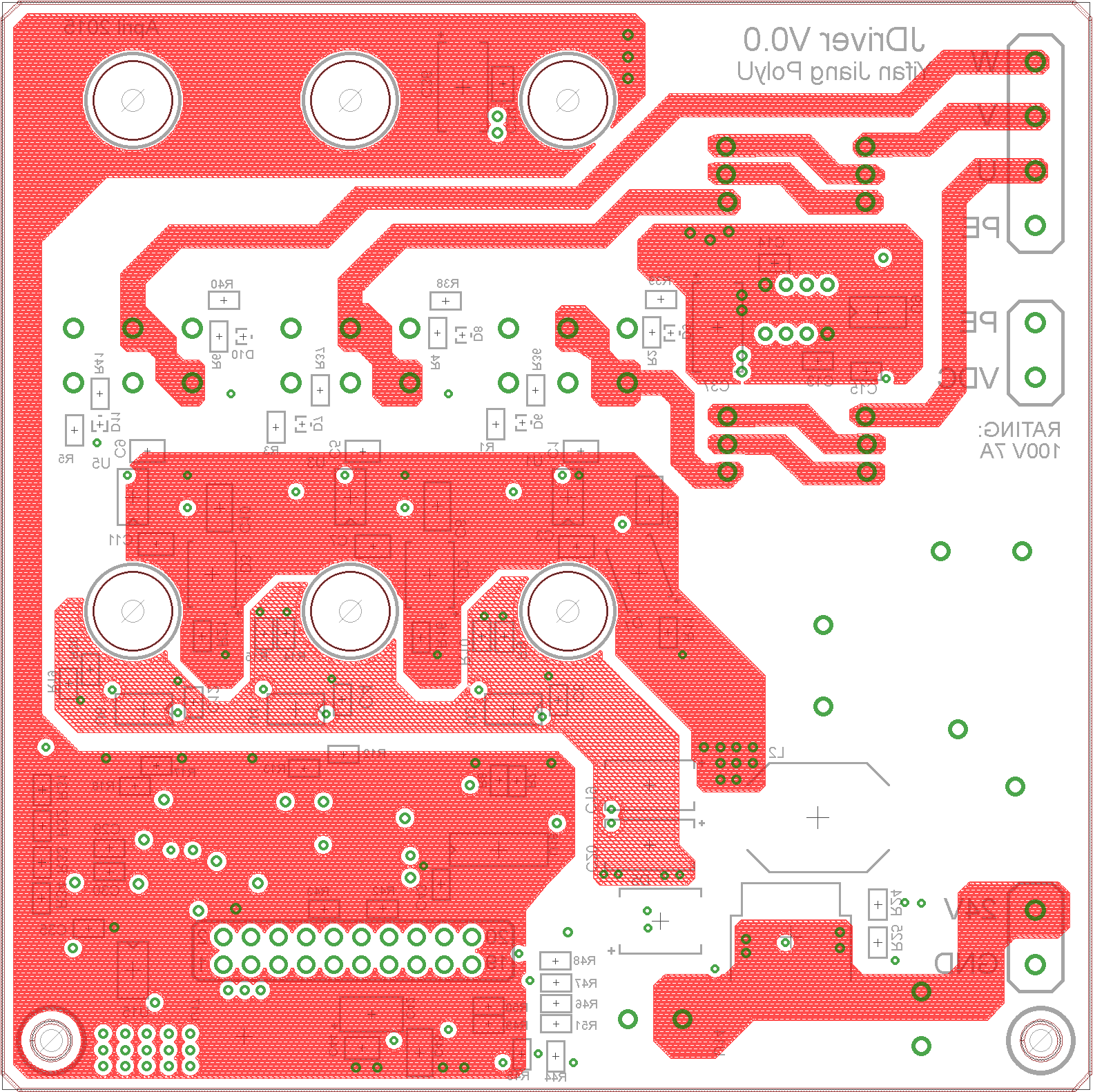
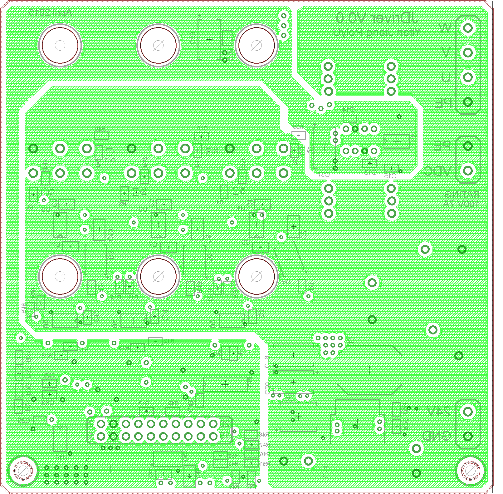
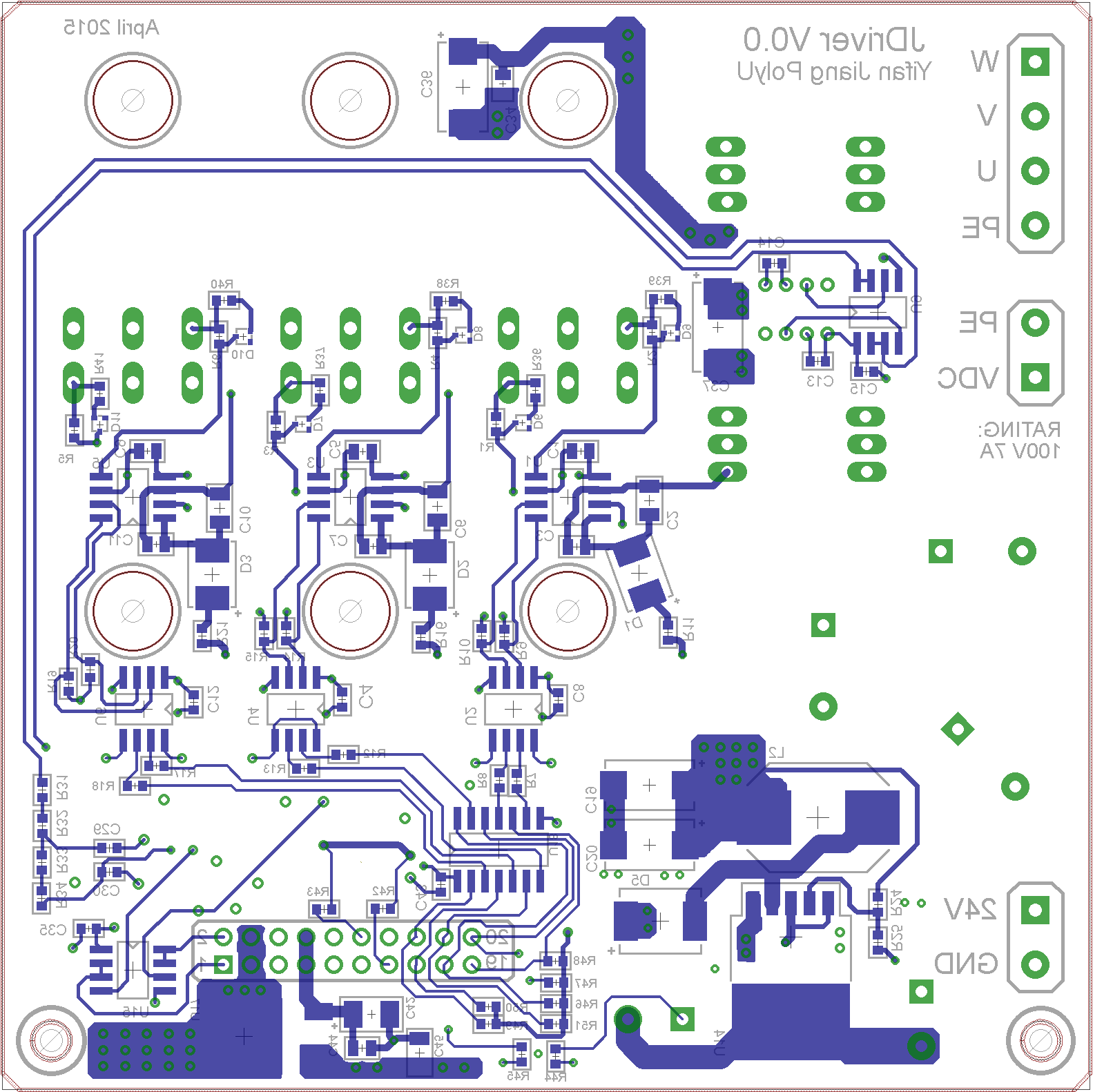
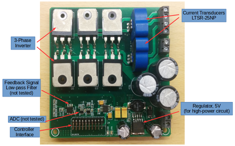
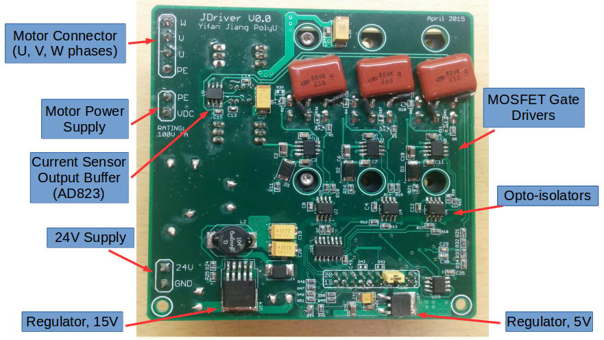
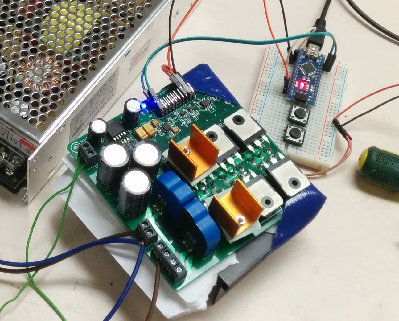
Fig.13 shows the finished motor driver in use, driving a brushed DC motor (only one of the 3 phases is used).
Leave a Comment